What Is Patterned Etching?
Patterned etching is a selective material removal process in which a protective mask — defined by photolithography, laser direct-write, or screen printing — is applied to the substrate surface to shield specific areas, while exposed regions are chemically or plasma-etched to a controlled depth. The mask material (photoresist, metal hard mask, or dielectric layer) is chemically resistant to the etchant, ensuring that only the unprotected areas are attacked. After etching, the mask is stripped to reveal the finished pattern. Wet chemical etching uses liquid etchants such as hydrofluoric acid (HF), buffered oxide etch (BOE), or potassium hydroxide (KOH) to isotropically or anisotropically remove material, while dry etching (ICP-RIE) uses plasma to achieve near-vertical sidewalls and sub-micron feature fidelity. Patterned etching is the foundational process for microfluidic channel fabrication, diffractive optical element production, MEMS device manufacturing, and any application requiring precise 2D or 2.5D features in glass or optical substrates without mechanical contact.
Process Capabilities
- Minimum Feature Size: 2 µm (photolithography); 5 µm (laser direct-write)
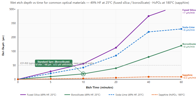
- Etch Depth Range: 0.1 µm – 500 µm (wet); 0.1 µm – 50 µm (dry / ICP-RIE)
- Depth Uniformity: ±0.5 µm across 150 mm substrate
- Sidewall Angle: 45° – 54.7° (isotropic wet); 80° – 90° (ICP-RIE dry)
- Etch Systems: HF / BOE (SiO₂) · KOH (Si) · H₃PO₄ (Al₂O₃) · ICP-RIE (all materials)
- Mask Types: Photoresist · Cr/Au hard mask · SiO₂ / Si₃N₄ dielectric mask
- Maximum Substrate Size: 200 mm diameter / 300 × 300 mm panel
Compatible Materials
| 1 | Fused Silica | Corning 7980 / Tosoh ES-2000 |
| 2 | Quartz Glass | SCHOTT Lithosil Q / Heraeus Suprasil 1 |
| 3 | Borosilicate Glass | PYREX 7740 / BOROFLOAT 33 |
| 4 | Soda-Lime Glass | Float / display-grade |
| 5 | Sapphire | C-plane / A-plane |
| 6 | Silicon | Float Zone / Czochralski |
| 7 | Glass-Ceramic | ZERODUR / PYROCERAM 9606 |
| 8 | Optical Glass | BK7 / N-BK7 |
| 9 | CaF₂ | UV-grade |
| 10 | Coated Glass | ITO / SiO₂ / Si₃N₄ thin film substrates |
| 11 | Technical Ceramics | Al₂O₃ / AlN |
Masking & Etching Strategy
- Photoresist Mask + HF/BOE: Standard for fused silica and borosilicate — fast, low cost, suitable for depth ≤ 50 µm
- Cr/Au Hard Mask + HF: For deep etching (> 50 µm) — metal mask survives long etch times where photoresist fails
- Laser Direct-Write + BOE: Maskless patterning — no photolithography tooling required, ideal for prototypes and custom patterns
- KOH Anisotropic Etching: For silicon substrates — produces crystallographic {111} sidewalls at 54.7°, highly repeatable
- ICP-RIE Dry Etching: Near-vertical sidewalls (80°–90°), sub-micron feature fidelity, suitable for all materials
- LACE (Laser + HF): Laser pre-modification accelerates HF etch rate by 100× in exposed zones — ultra-deep high-AR features
Typical Applications
- Microfluidic Channels: Wet-etched channels in fused silica and borosilicate for lab-on-chip devices
- Diffractive Optical Elements: Binary and multi-level phase gratings etched into fused silica
- MEMS Structures: Proof masses, cantilevers, and membrane features in glass and silicon substrates
- Micro-Lens Arrays: Isotropic etch-defined spherical micro-lens profiles in glass
- Alignment Marks & Fiducials: Permanent etched registration features for wafer bonding and lithography
- Optical Waveguide Structures: Ridge waveguides and photonic circuit features in glass substrates
Custom Specifications
We accept custom patterned etching orders based on GDS-II, DXF, or customer-supplied mask designs, supporting both prototype and production volumes. Custom parameters include mask material selection, etchant system, target depth and uniformity, sidewall angle, and multi-level etching for 3D profile features. Integrated workflows combining photolithography, etching, mask stripping, and post-etch inspection are available as a complete turnkey service. For microfluidic and MEMS applications, we also offer wafer bonding and dicing as downstream processes. All etched substrates are delivered with profilometry depth maps, feature dimension reports, and full process documentation.
Etch Depth vs Etch Time