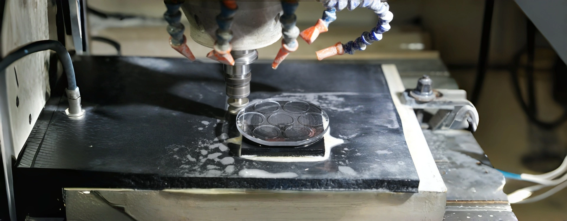
What Is Laser Microstructuring?
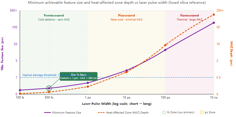
Laser microstructuring is a non-contact material processing technique in which focused ultrafast laser pulses — typically picosecond (10⁻¹² s) or femtosecond (10⁻¹⁵ s) duration — are used to ablate, modify, or restructure glass and optical substrates at the micron and sub-micron scale. Unlike nanosecond or continuous-wave lasers, which deposit energy thermally and cause melting and recast layers, ultrafast lasers transfer energy to the material faster than thermal diffusion can occur — a process known as cold ablation. This produces sharply defined features with negligible heat-affected zones, no micro-cracks, and no recast material. By scanning the focused laser spot across a programmed 3D toolpath, virtually any surface topography can be created: micro-channels, micro-pillars, diffractive gratings, moth-eye anti-reflection arrays, micro-lens arrays, and freeform optical surfaces. The process is entirely software-driven and requires no masks, molds, or chemical etchants, making it ideal for rapid prototyping and small-batch precision fabrication.
Process Capabilities
- Laser Sources: Picosecond (1064 nm / 532 nm / 355 nm) · Femtosecond (1030 nm / 515 nm / 343 nm)
- Minimum Feature Size: 1 µm (lateral) · 0.5 µm (depth increment)
- Depth Control Accuracy: ±0.5 µm per layer
- Surface Roughness (Ra) Post-Structuring: 50 – 200 nm (as-ablated); ≤ 10 nm (post-polished)
- Heat-Affected Zone (HAZ): < 500 nm (femtosecond); < 2 µm (picosecond)
- Maximum Structuring Area: 200 × 200 mm (stage travel)
- 3D Capability: Full volumetric structuring including subsurface bulk modification
Compatible Materials
| 1 | Fused Silica | Corning 7980 / Tosoh ES-2000 |
| 2 | Quartz Glass | SCHOTT Lithosil Q / Heraeus Suprasil 1 |
| 3 | Borosilicate Glass | PYREX 7740 / BOROFLOAT 33 |
| 4 | Sapphire | C-plane / A-plane |
| 5 | Optical Glass | BK7 / N-BK7 / N-SF11 |
| 6 | Glass-Ceramic | ZERODUR / PYROCERAM 9606 |
| 7 | Silicon | Float Zone / Czochralski |
| 8 | CaF₂ | UV-grade |
| 9 | Coated Glass | ITO / AR / dielectric-coated substrates |
| 10 | Thin Film Glass | 0.1 – 0.5 mm display-grade |
| 11 | Polymer Optics | PMMA / COP / COC (fs only) |
Microstructure Types
- Micro-Channels & Flow Cells: Sealed and open microfluidic channels, 5 – 500 µm wide
- Diffractive Optical Elements (DOE): Gratings, beam splitters, and phase plates with sub-µm period
- Moth-Eye AR Arrays: Sub-wavelength pillar arrays for broadband anti-reflection without coating
- Micro-Lens Arrays (MLA): Refractive and diffractive lens arrays for beam shaping and display optics
- Surface Texturing: Controlled roughness, hydrophobic/hydrophilic patterns, and tribological surfaces
- Bulk Refractive Index Modification: Waveguides, Bragg gratings, and 3D optical circuits inside glass
Typical Applications
- Microfluidics & Lab-on-Chip: Direct-write channel fabrication in fused silica without photolithography
- Optical Waveguides: 3D buried waveguide circuits in borosilicate and fused silica for photonic devices
- Anti-Reflection Surfaces: Moth-eye nanostructure arrays on sapphire and fused silica windows
- Beam Shaping Optics: Diffractive optical elements for laser beam homogenization and splitting
- Sensor Windows: Structured surfaces for LiDAR, IR, and UV sensor protective windows
- Biomedical Devices: Cell culture micro-well arrays and surface bio-functionalization patterns
Custom Specifications
We accept custom laser microstructuring orders based on customer-supplied CAD files, GDS-II layouts, or optical design specifications. Both surface structuring and bulk volumetric modification are available, with wavelength selection optimized for each material's absorption characteristics. Custom workflows include multi-pass depth profiling, grayscale ablation for freeform surface generation, and hybrid processes combining laser microstructuring with wet etching for high-aspect-ratio features. Post-structuring services — including confocal surface metrology, white-light interferometry inspection, AR coating, and cleanroom packaging — are available as part of a complete fabrication workflow. All structured substrates are delivered with full 3D surface maps and dimensional verification reports.
Feature Resolution vs Laser Pulse Width