Materials Used in Semiconductor Applications
We source and process high-purity glass materials suited for different cleanroom environments and bonding processes:
- Borosilicate Glass (e.g., Borofloat 33, MEMpax, Pyrex): Matches the thermal expansion of silicon (CTE ~3.3). This is the industry standard for Anodic Bonding in MEMS manufacturing.
- Fused Silica / Quartz: Ultra-high purity, extremely low thermal expansion, and excellent UV transmission. Used for high-temperature processes and lithography optics.
- Alkali-Free Glass: Prevents alkali ion contamination in sensitive electronic and TFT-LCD manufacturing processes.
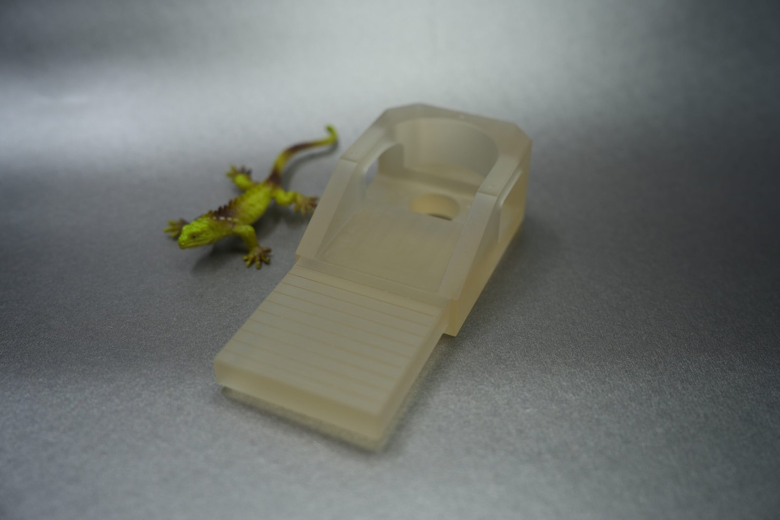
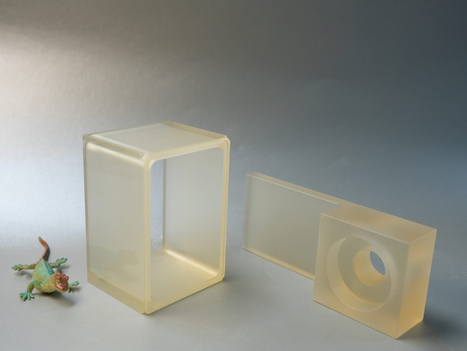
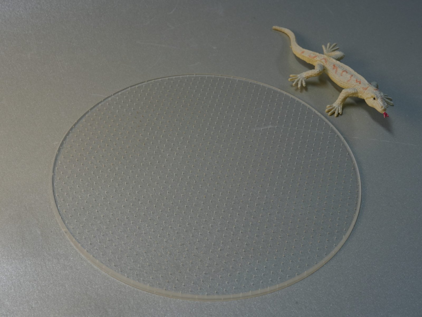
Products We Have Custom-Made (Real-World Cases)
We regularly supply custom glass components to semiconductor equipment manufacturers, research labs, and packaging facilities. Typical products include:
- Glass Carrier Wafers: Used to support thin, fragile silicon wafers during thinning and backside processing (Wafer-Level Packaging).
- Anodic Bonding Substrates: Custom-machined glass plates bonded to silicon for pressure sensors, accelerometers, and microfluidic devices.
- Dummy Wafers: Cost-effective glass wafers used for testing equipment, calibrating machines, and monitoring processes.
- Wafer Capping & Packaging Glass: Protective glass covers for CMOS image sensors and optoelectronics.
- Lithography & Inspection Windows: High-transmission, ultra-flat optical windows used in wafer metrology and inspection tools.
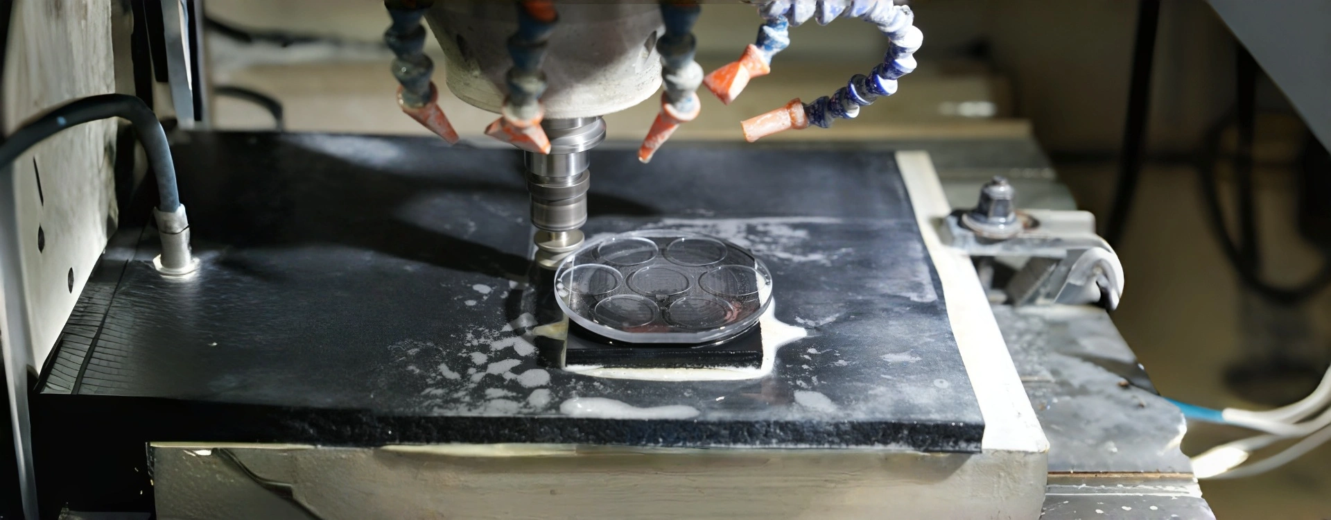
Our Precision Machining & Wafer Processing Capabilities
Semiconductor glass processing requires completely different standards than standard industrial glass. Our factory is equipped to handle:
- Wafer Coring & Sizing: Cutting custom diameters (2", 4", 6", 8", 12" or custom rectangular shapes).
- SEMI Standard Flats & Notches: Precision grinding of orientation flats or notches according to SEMI standards for automated handling.
- CMP (Chemical Mechanical Polishing): Achieving ultra-flat surfaces with extreme parallelity and sub-nanometer surface roughness (Ra) for bonding applications.
- Micro-Drilling & TGV: Precision laser or mechanical drilling for Through Glass Vias (TGV) and fluidic channels.
- Precision Dicing: Dicing large glass substrates into tiny, precise chips with zero edge chipping.
- Cleanroom Cleaning & Packaging: Ultrasonic cleaning and cleanroom vacuum sealing to ensure the glass is ready for your cleanroom environment.
Send Us Your Technical Specs
We understand that surface roughness, Total Thickness Variation (TTV), and bow/warp specs are critical for your success.
Need a custom batch? Send us your CAD drawings or PDF specifications. Please include your requirements for material type, dimensions, tolerances, and surface finish (Ra). Our engineering team will review the details and provide a fast, accurate quote.